Powered by Blogger.

Total Pageviews

I m on Twitter!

Thursday, April 12, 2012

VHDL code for Even Parity Generator

library ieee;
use ieee.std_logic_1164.all;

entity bejoy_ep is
port(x,y,z:in std_logic;
p:out std_logic);
end bejoy_ep;

architecture a of bejoy_ep is
begin
p<=((x xor y) xnor z);
end a;

VHDL code for Half Subtractor

library ieee;
use ieee.std_logic_1164.all;

entity bejoy_hs is
port (x,y,en : in bit ;
d,b : out bit; y1: inout bit);
end bejoy_hs;

architecture arc of bejoy_hs is
begin
process (en,y1)
begin
if en='1' then
d<= x xor y;
y1<= not (y);
b <= x and y1;
end if;
end process;
end arc;

Wednesday, April 11, 2012

VHDL code for 4x1 Multiplexer using structural style

library IEEE;
use IEEE.std_logic_1164.all;

entity bejoy_4x1 is
port(s1,s2,d00,d01,d10,d11 : in std_logic;
z_out : out std_logic);
end bejoy_4x1;

architecture arc of bejoy_4x1 is

component mux
port(sx1,sx2,d0,d1 : in std_logic;
z : out std_logic);
end component;

component or_2
port(a,b : in std_logic;
c : out std_logic);
end component;

signal intr1, intr2, intr3, intr4 : std_logic;
begin
mux1 : mux port map(s1,s2,d00,d01,intr1);
mux2 : mux port map(not s1,s2, d10,d11,intr2);
o1 : or_2 port map(intr1, intr2, z_out);
end arc;

library ieee;
use ieee.std_logic_1164.all;

entity mux is
port(sx1,sx2,d0,d1 :in std_logic;
z1,z2: inout std_logic;
z: out std_logic);
end mux;

architecture arc of mux is
begin
z1 <= d0 and (not sx1) and (not sx2);
z2 <= (d1 and (not sx1) and sx2);
z<= z1 or z2;
end arc;

entity or_2 is
port(a,b : in bit;
c : out bit);
end or_2;
architecture arc of or_2 is
begin
c<=a or b;
end arc;

VHDL code for Basic Gates

AND Gate

library ieee;

use ieee.std_logic_1164.all;

entity and_gate is

port (a,b : in std_logic ;

c : out std_logic);

end and_gate;

architecture arc of and_gate is

begin

c <= a and b; end arc;


OR Gate


library ieee;

use ieee.std_logic_1164.all;

entity or_gate is

port (a,b : in std_logic ;

c : out std_logic);

end or_gate;

architecture arc of or_gate is

begin

c <= a or b; end arc;


NOT Gate


library ieee;

use ieee.std_logic_1164.all;

entity not_gate is

port (a: in std_logic ;

b : out std_logic);

end not_gate;

architecture arc of not_gate is

begin

b <= not a; end arc;


NAND Gate


library ieee;

use ieee.std_logic_1164.all;

entity nand_gate is

port (a,b : in std_logic ;

c : out std_logic);

end nand_gate;

architecture arc of nand_gate is

begin

c <= a or b; end arc;


NOR Gate


library ieee;

use ieee.std_logic_1164.all;

entity nor_gate is

port (a,b : in std_logic ;

c : out std_logic);

end nor_gate;

architecture arc of nor_gate is

begin

c <= a nor b; end arc;


XOR Gate


library ieee;

use ieee.std_logic_1164.all;

entity xor_gate is

port (a,b : in std_logic ;

c : out std_logic);

end xor_gate;

architecture arc of xor_gate is

begin

c <= a xor b;

end arc;

Tuesday, April 10, 2012

Master Slave JK Flip Flop


library ieee;
use ieee.std_logic_1164.all;

entity master_slave_jk is
port(j,k,clk:in std_logic;q1,q1x,z1x:inout std_logic;
q2,q2x,z2x: inout std_logic);
end master_slave_jk;

architecture arc of master_slave_jk is
begin
process(clk)
begin

if clk='1' then

z1x<=(j and (not q2)) or ((not k)and q2);
q1<=z1x after 5 ns;
q1x<=not z1x after 5ns;

else

z2x<=(q1 and (not q2)) or ((not q1x)and q2);
q2<=z2x after 5 ns;
q2x<=not z2x after 5ns;

end if;
end process;
end arc;

VHDL code for T Flip Flop

library ieee;
use ieee.std_logic_1164.all;

entity bejoy_tff is
port(t,clk:in std_logic;q,q1,z:inout std_logic);
end bejoy_tff;

architecture arc of bejoy_tff is
begin
process(clk)
begin

if clk='1' then
z<=((t and (not q)) or ((not t) and q));
q<=z after 5ns;
q1<=not z after 5ns;

end if;
end process;
end arc;

VHDL code for Odd Parity Generator

library ieee;
use ieee.std_logic_1164.all;

entity bejoy_op is
port(x,y,z:in std_logic;
p:out std_logic);
end bejoy_op;

architecture a of bejoy_op is
begin
p<=((x xor y) xor z);
end a;

Monday, April 9, 2012

VHDL code for 3x8 Decoder

library ieee;
use ieee.std_logic_1164.all;

entity bejoy_3x8 is
port(a,b,c:in std_logic;
d0,d1,d2,d3,d4,d5,d6,d7:out std_logic);
end bejoy_3x8;

architecture arc of bejoy_3x8 is
begin
d0<= (not a) and (not b) and (not c);
d1<= (not a) and (not b) and c;
d2<= (not a) and b and (not c);
d3<= (not a) and b and c;
d4<= a and (not b) and (not c);
d5<= a and (not b) and c;
d6<= a and b and (not c);
d7<= a and b and c;
end arc;

VHDL code for JK Flip Flop

library ieee;
use ieee.std_logic_1164.all;

entity bejoy_jkff is
port(j,k,clk:in std_logic;q,q1,z:inout std_logic);
end bejoy_jkff;

architecture arc of bejoy_jkff is
begin
process(clk)
begin

if clk='1' then
z<=(j and (not q)) or ((not k) and q);
q<=z after 5ns;
q1<=not z after 5ns;

end if;
end process;
end arc;

Sunday, April 8, 2012

VHDL code for Full Adder using structural style

library IEEE;
use IEEE.std_logic_1164.all;

entity bejoy_fa is
port(In1,In2,c_in : in std_logic;
sum, c_out : out std_logic);
end bejoy_fa;

architecture arc of bejoy_fa is

component half_adder
port(a,b : in std_logic;
sum, carry : out std_logic);
end component;

component or_2
port(a,b : in std_logic;
c : out std_logic);
end component;

signal s1, s2, s3 : std_logic;

begin

H1: half_adder port map(a=>In1, b=>In2, sum=>s1, carry=>s3);

H2: half_adder port map(a=>s1, b=>c_in, sum=>sum, carry=>s2);

O1: or_2 port map(a=> s2, b=>s3, c=>c_out);

end arc;

entity half_adder is

port (a,b : in bit ;
sum,carry : out bit);

end half_adder;

architecture arc of half_adder is

begin

sum<= a xor b;
carry <= a and b;

end arc;

entity or_2 is

port (a,b : in bit ;
c : out bit);

end or_2;

architecture arc of or_2 is

begin

c<= a or b;

end arc;

100 Watt Audio Power Amplifier


This is an exceptionally well designed amplifier, with a lot of power reserve, high fidelity, low distortion, good S/N ratio, high sensitivity, low consumption and full protection. Having all these almost ideal characteristics this amplifier is likely to become the basic building block of your future high fidelity system, or it can also become the element that will upgrade your existing system.


How it Works


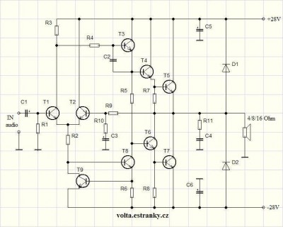
The circuit works from a symmetrical ñ 40 VDC power supply and draws a maximum current of 2.6 A. The input circuit of the amplifier is a differential amplifier built around Q4 and Q5 that employ DC feedback thus preventing any DC voltage from appearing across the speaker with the usual destructive results. Q11 acts as a current source and ensures that the input stage draws a constant current of 1 mA.

The signal which appears as a voltage drop across the resistor connected in series with the collector of Q4 is used to drive the DARLINGTON pair Q3, Q2 which together with the constant current source of 7 mA that is Q10, form the driver stage. This stage operates in class A and is driving the complementary output stage Q1, Q9. The transistor Q7 is used to balance the circuit at different temperatures and must be mounted on the heatsink between the out put transistors. The feedback loop which consists of R8, R9, C2, C3 provides AC stability to the circuit. The circuit also incorporates a protection stage that makes it virtually indestructible. This protection circuit is built around Q6, Q8. If for whatever reason the output remains connected on one supply rail and the common the output is also protected from high DC voltages that could burn the speakers. The supply rails should be protected by 2 A fuses for the 8 ohm version and 3 A for the 4 ohm.


Technical Specifications - Characteristics


Output power (f=1 KHz, d=0.5 %): 100 W in 8 ohm

Supply voltage: ................  40 V

Quiescent current: ............. 50 mA

Maximum current: ............... 2.6 A

Sensitivity: . 600 mV

Frequency response: ............ 10-35000 Hz (-1 dB)

Distortion HD: ................. 0.01 %

Intermodulation dist.: ......... 0.02 %

Signal/noise: 83 dBConstruction


PLEASE READ THIS BEFORE YOU START CONSTRUCTION


To cater for those who wish to use 4 ohm speakers with this amplifier the Kit includes the necessary components for both versions. The components that differ are R3,4,17 and 23. If you build the 8 ohm version then you must also include in the circuit R28 and D7, D8 which are not used in the 4 ohm version. As you see all the components are already marked on the component side of the p.c. board.

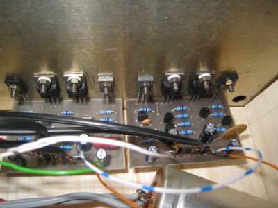
The construction is made this way much simpler. Start the construction from the pins and the jumper connections, continue with the resistors and the capacitors and last solder in place the semiconductors. Check each resistor before soldering it, to see if its colours match those in the component list. Be careful with the electrolytic capacitors because their polarity should be respected. The polarity of those capacitors is marked on their bodies and on the component side of the p.c. board.

NOTE: On the p.c. board next to R2, R16 are marked two other resistors which do not appear in the circuit diagram but are included in the components. They are of 1 ohm 2 W (brown, black, gold) and must be included in the circuit. Take care when you are soldering the semiconductors because if you overheat them they can be damaged.

The output transistors should be mounted on the heatsink that is included in the kit. Take care not to short circuit them with the heatsink and we recommend that you use some HTC between the transistor body and the sink in order to improve heat dissipation. Follow the diagram for the mounting of the power transistors as it shows clearly how to insert the insulators and the screws. Q7 should be made to touch the heatsink and is a good idea to use a bit of HTC between its casing and the surface of the heatsink.

When you finish the construction of your project clean the board thoroughly with a solvent to remove all flux residues and make a careful visual inspection to make sure there are no mistakes, components missing and short circuits across adjacent tracks on the board. If everything is OK you can make the following connections: Input: 3 (signal), 5 (common) Output: 7 (signal), 6 (common) Supply: 1 (-40 VDC), 2 (+40 VDC) 5 (0 VDC)


Connect a milliammeter in series with the power supply, short the input of the amplifier, turn the power ON and adjust the trimmer P1 so that the quiescent current is about 50 mA. When you finish this adjustment remove the shunt from the input and connect the output of a preamplifier to it. Connect the pre amplifier to a suitable source and turn everything ON.

The signal should be heard from the speakers clear and undistorted. First of all let us consider a few basics in building electronic circuits on a printed circuit board. The board is made of a thin insulating


material clad with a thin layer of conductive copper that is shaped in such a way as to form the necessary conductors between the various components of the circuit. The use of a properly designed printed circuit board is very desirable as it speeds construction up considerably and reduces the possibility of making errors. Smart Kit boards also come pre-drilled and with the outline of the components and their identification printed on the component side to make construction easier. To protect the board during storage from oxidation and assure it gets to you in perfect condition the copper is tinned during manufacturing and covered with a special varnish that protects it from getting oxidised and makes soldering easier. Soldering the components to the board is the only way to build your circuit and from the way you do it depends greatly your success or failure. This work is not very difficult and if you stick to a few rules you should have no problems. The soldering iron that you use must be light and its power should not exceed the 25 Watts. The tip should be fine and must be kept clean at all times. For this purpose come very handy specially made sponges that are kept wet and from time to time you can wipe the hot tip on them to remove all the residues that tend to accumulate on it.

 DO NOT file or sandpaper a dirty or worn out tip. If the tip cannot be cleaned, replace it. There are many different types of solder in the market and you should choose a good quality one that contains the necessary flux in its core, to assure a perfect joint every time.

DO NOT use soldering flux apart from that which is already included in your solder. Too much flux can cause many problems and is one of the main causes of circuit malfunction. If nevertheless you have to use extra flux, as it is the case when you have to tin copper wires, clean it very thoroughly after you finish your work. In order to solder a component correctly you should do the following:


  • Clean the component leads with a small piece of emery paper. - Bend them at the correct distance from the component body and insert the component in its place on the board.


  • You may find sometimes a component with heavier gauge leads than usual, that are too thick to enter in the holes of the p.c. board. In this case use a mini drill to enlarge the holes slightly. Do not make the holes too large as this is going to make soldering difficult afterwards.


  • Take the hot iron and place its tip on the component lead while holding the end of the solder wire at the point where the lead emerges from the board. The iron tip must touch the lead slightly above the p.c. board.


  • When the solder starts to melt and flow, wait till it covers evenly the area around the hole and the flux boils and gets out from underneath the solder. The whole operation should not take more than 5 seconds. Remove the iron and leave the solder to cool naturally without blowing on it or moving the component. If everything was done properly the surface of the joint must have a bright metallic finish and its edges should be smoothly ended on the component lead and the board track. If the solder looks dull, cracked, or has the shape of a blob then you have made a dry joint and you should remove the solder (with a pump, or a solder wick) and redo it.


  • Take care not to overheat the tracks as it is very easy to lift them from the board and break them.


  • When you are soldering a sensitive component it is good practice to hold the lead from the component side of the board with a pair of long-nose pliers to divert any heat that could possibly damage the component.


  • Make sure that you do not use more solder than it is necessary as you are running the risk of short-circuiting adjacent tracks on the board, especially if they are very close together.


  • When you finish your work cut off the excess of the component leads and clean the board thoroughly with a suitable solvent to remove all flux residues that still remain on it.

If it does not work


Check your work for possible dry joints, bridges across adjacent tracks or soldering flux residues that usually cause problems. Check again all the external connections to and from the circuit to see if there is a mistake there.


  • See that there are no components missing or inserted in the wrong places.


  • Make sure that all the polarised components have been soldered the right way round. - Make sure the supply has the correct voltage and is connected the right way round to your circuit.


  • Check your project for faulty or damaged components. If everything checks and your project still fails to work, please contact your retailer and the Smart Kit Service will repair it for you.


L1 : 10 turns with wire 0,5mm turned on a restistor of 1W


If you use a 4Ohm speaker you will place R3,4,17,23 at the board.


If you use a 8Ohm speaker you will place D7 D8 and R28.


For R2 and R16 if you don't find a 0,47Ohm place two of 1 Ohm parallel.


R16 must be 0,47Ohm...the 1Ohm must be a typographical error, take care of this, i haven't tested it.

VHDL code for Half Adder

library ieee;
use ieee.std_logic_1164.all;

entity bejoy_ha is

port (a,b : in bit ;

s,c : out bit);

end bejoy_ha;

architecture arc of bejoy_ha is

begin

s<= a xor b;
c <= a and b;

end arc;

50 watts transistor amplifier

The amplifier and speakers that can handle medium-power is designed to provide a strictly amateur. Accidental overloads can damage the speakers, it is not appropriate for small systems.

What amp settings do not contain an element of the first connection wiring must be careful to work with.
Characteristics of the transistor, the fan or heat sink is cooled enough to find out if you need to focus!

Tech. parameters:
Power: + - 28V
Power: 50W / 4 ohms
Input sensitivity: 250mW of
Input resistance: 50 kOhm
Frequency range: 30Hz to - 30kHz

Optimal mobile recording portable player to another amplifier Multi Media.


Here, the schematics this power amplifier


List of components:
R1, R2, R9 - 56K
R3 - 3K3
R4, R6 - 100R
R5 - 220R
R7, R8 - 120R
R10 - 1K
R11 - 1R
C1 - in 1µF / 35V
C2 - 33P - Ceramics
C3 - the 100µF/35V
C4 - 100 N (220N) - Ceramic
C5, C6 - 4.7 UF / 35V
D1, D2 - 1N4007
T1, T2, T9 - BC546
Q3 - BC640
T4 - BD139
T5, T7 - BD711
T6 - BD140
T8 - BC639

Following the DC voltage amplifier and limiter speaker protection is needed.


source: http://www.volta.estranky.cz/clanky/zesilovace-a-predzesilovace/tranzistorovy_zesilovac_50_W.2.html

Saturday, April 7, 2012

Fet Buffer for amplifiers


source: http://cappels.org/dproj/edfet/edfet.html

The EDFET drives like a FET, but with the bias stability of bipolar. Amps of output current can be controlled by milliamps of input current. The current gain is a design choice dictated by bandwidth. Two of things you have to consider when adding a power output stage to an op-amp circuit are the frequency response and the cross-over distortion in that stage.

This is especially true with wide band amplifiers, where the unity gain crossover needs to be at several hundred kilohertz. The stage is driven much the same as a complimentary pair output stage, but with the current gain that comes with using FETs., and with feedback within the output stage that that extends the buffer's bandwidth and regulates the quiescent current. More predictable operation allows the designer to design a circuit lower overall power dissipation and better closed loop stability.


Fet Buffer for amplifiers


The EDFET complimentary buffer is made up of a pair of unity gain buffers, one that drives in the positive direction and the other that drives in the negative direction. Pictured above is the positive driving half of the output stage.

Gain to make the output signal track the input signal comes from inverting transistor, Q1. The input signal is applied to the emitter of Q1 and the output of the amplifier is raised one diode drop to match the forward base-emitter drop of Q1, by diode connected transistor Q2. The buffer's offset is determined by the log of the magnitude of the mismatch in the emitter currents in Q1 and Q2, and it is directly proportional to the absolute temperature.

Since the saturation current usually isn't published for the transistors this expression is only usefully for appreciating the dependence of junction voltage on current and temperature. You can come up with your own value of I0 for a given transistor if you know all the other parameters and solve the above formula for I0. By the way, since, for most practical uses, you will be running at more than a thousand times the saturation current, the "+1" term can be dropped from practical calculations.

As an example, for the audio amplifier using a EDFET buffer shown in Figure 1. The following assumptions are applied: The maximum output voltage is 5 VDC with respect to ground, the power supply (VA) is 12 VDC, the maximum gate voltage is 8 VDC, the input capacitance, Ciss of the BUZ73 is 500 pf, and an...
http://cappels.org/dproj/edfet/edfet.html

Discrete Buffer: Diamond Buffer
Discrete Buffer: JISBOS Buffer

VHDL code for 1x2 Demultiplexer

library ieee;
use ieee.std_logic_1164.all;

entity bejoy_1x2 is
port(d,s:in std_logic;

z0,z1:out std_logic);
end bejoy_1x2;

architecture arc of bejoy_1x2 is
begin
z0 <= d and (not s);
z1 <= (d and s);
end arc;

Design Buffers: Improved unity-gain follower delivers fast, stable response


Robert A Pease, National Semiconductor Corp -- EDN, June 27, 2011


Heavy load capacitance can cause the output of a unity-gain follower—an operational amplifier with direct feedback to the inverting input (Fig 1)—to ring and oscillate. The LM110 follower, for example, normally drives a 50-pF load without problems, but it does not drive 500 pF stably—high capacitance significantly modifies the open-loop output impedance, reducing the phase margin to zero and causing oscillation.


You can easily eliminate such instability problems by adding a capacitor and resistor in series across the op amp's inverting and noninverting inputs. This solution can also greatly improve a follower's slew rate.


Analyze the problem


In general, increasing the ac noise gain of an op amp's feedback network improves capacitive-load tolerance. A common gain-increasing strategy adds R2~RF/10 to the circuit shown in Fig 2. (A moderate-value capacitor, C2, usually inserted in series with R2, prevents the dc noise gain from also increasing and degrading dc-offset, drift and accuracy specifications.)


Improved unity-gain follower delivers fast, stable response figure 2

If the op amp has a 1-MHz gain-bandwidth product and R1=RF, the closed-loop frequency response will be 500 kHz. Inserting R2=RF/10 drops this frequency response to 90 kHz, where the amplifier usually tolerates a much larger capacitive load. AC noise gain equals (RF/ R1)+(RF/R2)+1, and dc noise gain is (RF/R1)+1.


Improved unity-gain follower delivers fast, stable response figure 2


You can also increase ac noise gain by installing R3 and C3 instead of R2 and C2. The resulting value is


[1+(RF/R1)][(R++R3)/R3]+(RF/R3).


In the simplest case, R1 forms an open circuit, and ac noise gain equals


(R+/R3)+(RF/R3)+1.


Therefore, you can raise ac noise gain by using a low value for R3 and a high value for R+ and/or RF.


The solution follows


For the particular case of a unity-gain follower, RF is normally 0O as shown in Fig 3. According to the foregoing general analysis, if the value of RS is low, ac noise gain is (R4/R5)+1, so you can increase ac noise gain—and therefore stability—by adding a large R4 and a small R5. (A large and constant RS can make R4 unnecessary; ac noise gain is then (RS/R5)+1.)


Improved unity-gain follower delivers fast, stable response figure 3

With LM110/LM310s, for example, 10k is an appropriate value for R4. Using R5 = 3.3k and C5 = 200 pF, the LM110 stably drives capacitive loads up to 600 pF.


Technique speeds followers
You can also wire the resistor/capacitor combination across an op amp's inputs to increase the follower's slew rate. For example, an LF357 op amp's decompensation with a small internal capacitor normally requires gains higher than five to maintain stability (Fig 4). But the LF357 fits unity-gain-follower applications as easily as the LF356 (which is identical to the 357 except for the 356's internal compensation) and achieves better results. When source resistance is less than 1k, both the LF357 and 356 provide fast, stable responses, but the 357 has a 50V/µsec slew rate (typical) compared with 12V/µsec for a 356.


Improved unity-gain follower delivers fast, stable response figure 4


The LM349 decompensated quad op amp furnishes a bipolar input stage with a finite bias current (200 nA max). For best results in this application, add the resistor that controls the noise gain equally to the inverting and noninverting inputs as shown in Fig 5. With this circuit, the LM349 can slew at 2V/µsec typ and handles audio signals much faster—and without distortion—than the compensated LM348 (which, at 0.5V/µsec, slews only as fast as the general-purpose LM741). You can use the same approach for an LM101 by employing a 5-pF damping capacitor.


Improved unity-gain follower delivers fast, stable response figure 5


Watch for problems

While inserting a resistor/capacitor combination across the inputs gives faster slewing, the circuit's bandwidth could degrade if source impedance (RS) increases. In addition to guarding against bandwidth problems, make sure ac noise doesn't reach an objectionable level when you raise ac noise gain. Although most modern op amps exhibit low noise, raising that noise gain to 10 can significantly increase output noise.


If the series capacitor across the op amp's inputs is larger than necessary for stability and high slew-rate purposes, noise increases unnecessarily. In general, choose the minimum capacitance for the circuit in Fig 3 according to the following formula (where fV = op amp's unity-gain bandwidth):


C5min = 4[1+(R4/RS)]/2pR5fV=(R4+R5)/(p/2)fV(R5)2. To allow for tolerance variations, make C5's circuit value two or three times C5min.

source: http://www.edn.com/article/518641-Improved_unity_gain_follower_delivers_fast_stable_response.php

VHDL code for Full Subtractor

library ieee;
use ieee.std_logic_1164.all;

entity bejoy_fs is
port(x,y,bi: in bit; b2,do,bo: out bit; d,b: inout bit);
end bejoy_fs;

architecture arc of bejoy_fs is
begin
d<=x xor y;
b<=x and (not y);
do<=bi xor d;
b2<=bi and (not b);
end arc;

VHDL code for 4 bit Gray to Binary converter

library ieee;
use ieee.std_logic_1164.all;

entity bejoy_g2b is
port(g:in std_logic_vector(3 downto 0);

b:inout std_logic_vector(3 downto 0));
end bejoy_g2b;


architecture a of bejoy_g2b is
begin

b(3)<=g(3);
b(2)<=b(3) xor g(2);
b(1)<=b(2) xor g(1);
b(0)<=b(1) xor g(0);
end a;

Friday, April 6, 2012

VHDL code for 4 bit Binary to Gray code converter

library ieee;
use ieee.std_logic_1164.all;

entity bejoy_b2g is
port(b:in std_logic_vector(3 downto 0);

g:out std_logic_vector(3 downto 0));
end bejoy_b2g;

architecture a of bejoy_b2g is
begin

g(3)<=b(3);
g(2)<=b(3) xor b(2);
g(1)<=b(2) xor b(1);
g(0)<=b(1) xor b(0);
end a;

VHDL code for SR Flip Flop

library ieee;
use ieee.std_logic_1164.all;

entity bejoy_rsff is
port(s,r,clk:in std_logic;q,q1,z:inout std_logic);
end bejoy_rsff;

architecture arc of bejoy_rsff is
begin
process(clk)
begin

if clk='1' then
z<=s or ((not r) and q);
q<=z after 5ns;
q1<=not z after 5ns;

end if;
end process;
end arc;

Ads By Sponsers